PSoC5LP Lab 01: Switch and LED Control without C Code
Objective
- Understand how to configure and control hardware resources within the PSoC 5LP device using the design tool.
- Implement basic digital I/O functionality (button and LED control) using PSoC Creator.
- Observe internal hardware routing to achieve functionality without writing C code.
Overview
The PSoC 5LP (Programmable System-on-Chip) is a flexible and powerful microcontroller architecture from Cypress Semiconductor that combines a CPU with configurable analog and digital blocks. Its unique internal hardware routing allows complex digital and analog functions to be implemented without CPU intervention or traditional C code.
This makes it ideal for applications where reduced CPU load or low-power operation is critical. The PSoC's programmability also simplifies designs by integrating multiple functions (such as timers, PWM, and logic gates) into a single chip.
In this lab, users explore controlling an LED with a button using PSoC Creator’s graphical interface, without any C code. This exercise introduces the fundamental concepts of using PSoC's digital input/output pins, internal routing, and basic peripheral configuration. The goal is to demonstrate how configurable logic in the PSoC enables hardware components to communicate without relying on the CPU, thereby creating efficient, low-latency systems.
The flexible pin assignments and routing paths are critical, allowing the same chip to be used in various applications without additional components. This lab also highlights how using schematics and the Pin Assignment tool in PSoC Creator helps manage the I/O pins and internal configurations.
Required Reading Materials
Required Components
If you use the Cypress CY8CKIT-059 Kit, the onboard LED and button will be used in this lab.
The following components are required for this lab.
 |
Push Button (Optional, can use onboard components) | x 1 |
| Resistor 200ohm (if using an external LED) | x 1 | |
| Red LED (or onboard LED) | x 1 |
Circuit / Schematic
Cypress CY8CKIT-059 Kit
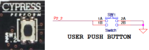
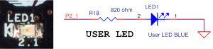
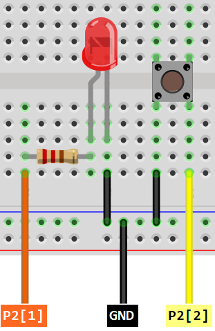
The CY8CKIT-059 board contains a single push button and a blue User LED. The push button is connected to GND and to the P2[2] pin on the PSoC 5LP device. The blue user LED is connected with a resistor and to P2[1] of the target PSoC 5LP device.
EagleSoC Development/Mini Board
Procedure
Creating a New Project
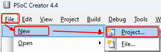
- Launch PSoC Creator.
- Go to File ➤ New ➤ Projects….
- Select the correct PSoC5L microcontroller chip number.
- If you are using PSoC Creator for the first time or working with a different PSoC board than before, select Launch Device Selector to choose the appropriate PSoC5LP chip model.
For CY8CKIT-059 Kit: CY8C5888LTI-LP97 device.
PSoC Creator will remember the last PSoC CPU model number you used. If you use the same type of PSoC board, then you can select it.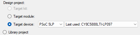
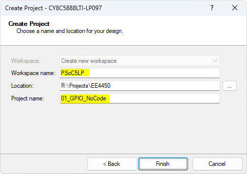
- Click next after selecting the CPU model number. Select Empty Schematic, then click Next.
- Edit the name of the Project and Workspace.
Adding PSoC Creator Components
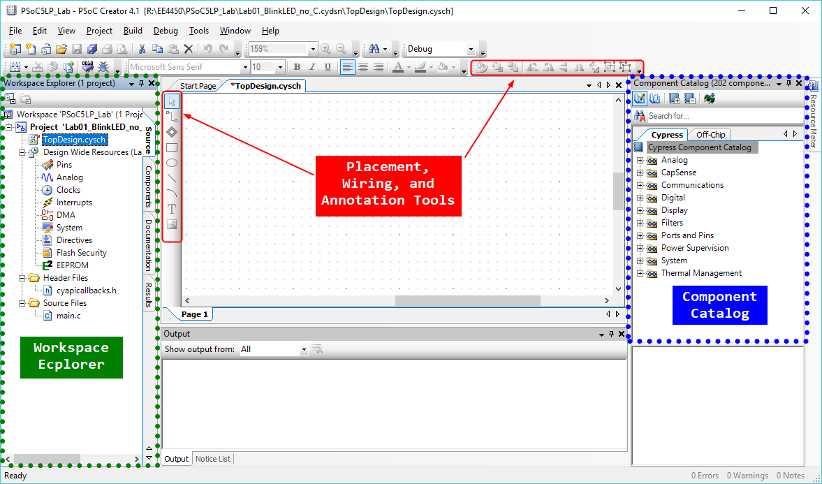
After you create a project, PSoC Creator opens the TopDesign.cysch tab with an empty schematic. You need to add some components to TopDesign.cysch. On the right side of the PSoC Creator window, you can see a tree-structure panel called the "Component Catalog", which has Cypress and Off-Chip tabs for component selection.
- Cypress: Developed by Cypress for use in designs.
- Off-Chip: This is for documenting connections, primarily for reference.
Adding Components:
- Select Digital Input Pin and Digital Output Pin from the Ports and Pins catalog under the Cypress tab.
- Drag the components to the schematic as shown on the following diagram:
- Place input components (like switches) on the left.
- Place output components (like LEDs) on the right.
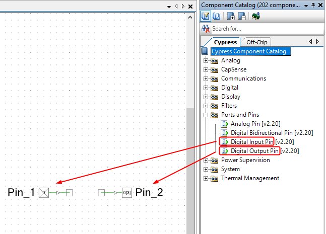
When you drag components into the schematic, always place Input components on the left and Output components on the right.
Configure the Components
In your next step, you will need to configure these components.
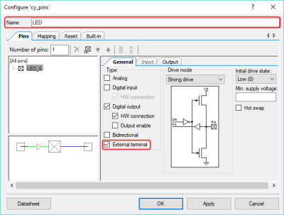
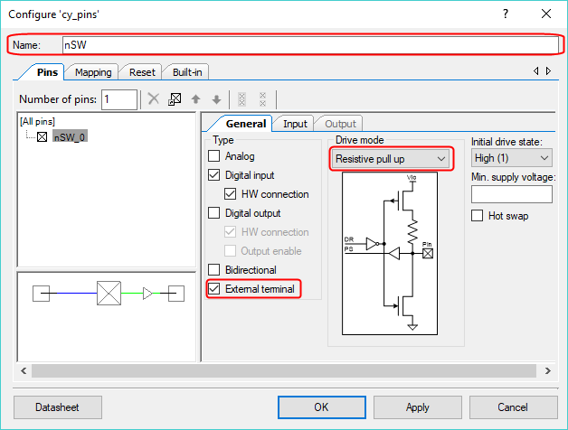
- Double-click on the Pin_1 component, the input pin. You will get the component configuration window, where you can set all the various parameters that define the part at build time.
- Change the component name to nSW.
- Select the External terminal checkbox to show the terminal pin and enable the connections to Off-Chip Components in the schematic.
- Change Drive mode to Resistive pull-up.

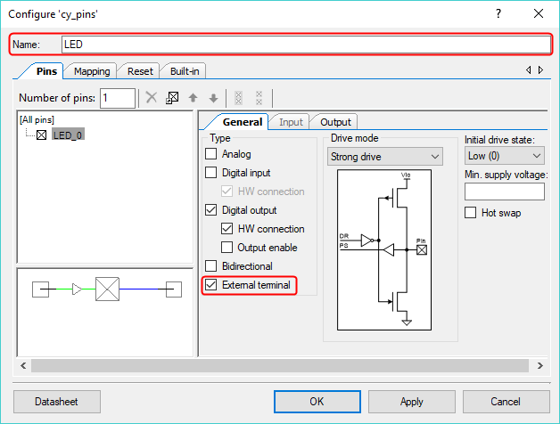
- Perform the same procedure for the output pin, but leave the drive mode at its default setting. Double-click on the Pin_2 component, the output pin.
- Change the component name to LED.
- Select the External terminal checkbox to show the terminal pin.
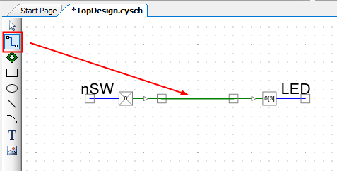
Wiring
In this lab, we want to turn on the LED by pressing the push button, so you need to connect the input and output components.
- Single-click on the Wire Tools
 button to draw one wire connection.
 - Double-click the schematic to start or end a wire-drawing process.
- Double-click on the Wire Tools button to draw multiple wires at once.
- Press the [ESC] key to quit drawing wires.
Drawing an External Circuit on the Schematic
Drawing the complete external circuit on the schematic will help you quickly understand input and output signals.
Open the Off-Chip tab on the Component Catalog panel, then drag external components into your schematic, as shown in the following diagram.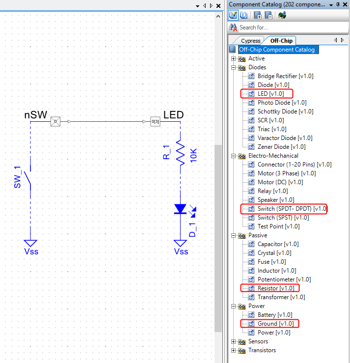
The schematic representation of Vss (Ground), 10K Resistor R_1, LED D_1, and Switch (SPST) SW_1 is just 'visual aids'. These visual aids are:
- available Off-Chip library component tab
- is shown in blue
These components are not considered in the PSoC programming stage. All components shown in blue are not used during the build.
The Green wires are digital connections. They connect components via an internal routing path to transmit signals.
The Blue wires and Blue components are off-chip documentation components. They are used to illustrate circuitry external to PSoC devices only. It can help you and other engineers understand the circuit quickly, but it is not used to build the project.
Pin Assignment
| Device | Port.Pin | Direction | Drive Mode |
|---|---|---|---|
Before building the code, the last thing to do is assign these logical pins to a physical pin on the PSoC 5LP device. To do this, open the Design Wide Resources file (.cydwr) from the Workspace Explorer on the left side of the window. You will get a similar pin assignment window as shown in the following figure: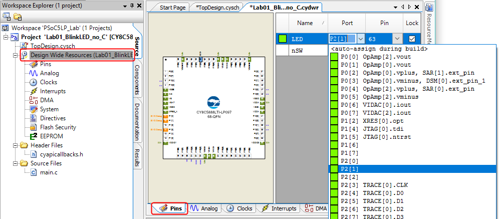
On the right side, there is a list of pin objects, port pins, and physical PINs. If you do not assign a pin to a physical port, the PSoC Creator will do it. In this Lab, the LED is connected to port 2, pin1, and the push button is attached to port 2, pin2. So, you have to assign P2[1] to LED and P2[2] to nSW.
Building the code and Programming
No additional software is needed in main.c for this experiment. Therefore, you can build the project using the Build menu or the ![]() Build icon. The Output panel shows the build results. Any errors will stop the build process, and messages identifying these problems will be displayed in the Output panel.
Build icon. The Output panel shows the build results. Any errors will stop the build process, and messages identifying these problems will be displayed in the Output panel.
To program the PSoC with the newly built firmware, connect the PSoC board to the PC using the USB cable. Load the program using either the Debug➤Program selection or the following ![]() Program icon. The programming status is also shown in the Output panel.
Program icon. The programming status is also shown in the Output panel.
When programmed, you can press the push button to observe the LED's status.
Exercises
Exp #01: Toggle the LED
Design a hardware that toggles the LED each time the button is pressed.
Using same external circuit and connections that were previously used in the Lab. Create a new project and draw the schematic file as shown in the following diagram.
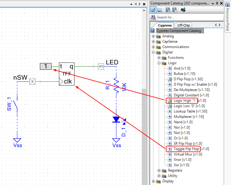
Build the project and program the code to the PSoC board, then press the button to observe the LED changing.
Questions:
- Does the LED change status when you press the button? Explain why.
- Redo this exercise by using D Flip Flop (with logic gates) instead of Toggle Flip Flop, and modify your TopDesign to change the LED status when you press the button. Show your TopDesign on the report.
Questions
- Is the LED on when the button is pressed and off when it is released? If not, can you just add one more component from the Component Catalog to the Schematic file in the PSoC Creator without changing any physical hardware outside the device? Explain.
- Why must the Drive mode in nSW (Digital Input Pin) be a Resistive Pull Up? Change the Drive mode to High Impedance Digital, then program the PSoC and see what happens. Explain.
- Most microcontrollers do not have configurable routing paths to connect internal components. How can this lab be implemented in these MCUs? Show your solutions using the Flowchart or pseudocode in the report.